Breakthroughs in key industry of the future
The Swiss Light Source (SLS), the circular architectural landmark of PSI in Villigen, is known as a state-ofthe-art measuring and reading device. It uses X-rays to make crystal structures or other minute structures visible in high resolution. Amazingly, it is also possible to write or engrave with this light source.
Chip production in the nanometre range
According to Mirko Holler, researcher at the Laboratory for Macromolecules and Bioimaging, using photolithography in chip production is essentially the same concept as the traditional printing process with stone plates, “except the stone is now pure silicon.” However, there is a big difference. In conventional printing, you cannot go beyond the limits of what is visible to the naked eye, whereas chip production has long since moved into dimensions that are barely imaginable and perhaps even impossible to produce.
This is because orders of magnitude in the low nanometre range cannot be achieved with visible light, as its wavelengths are too long for this. And the trend is towards even shorter wavelengths. In recent years, chip production has reached the extreme UV (EUV) range of the light spectrum, which ultimately merges into Xrays. The chip industry has already “invested billions” in EUV lithography, and scanners, which transfer chip patterns to silicon, can currently achieve a resolution of up to 13 nanometres. However, newer machines will be able to reach 8 nanometres.
Extension of conventional EUV lithography
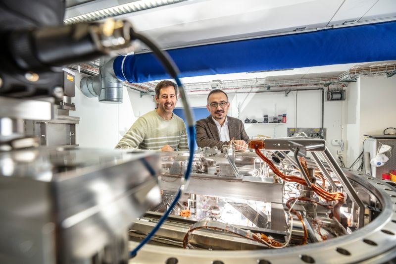
Yasin Ekinci, Head of the Laboratory for X-ray Nanoscience and Technologies, and his team at PSI have developed a method that uses EUV to advance into physically “impossible” orders of magnitude. The team has taken conventional EUV lithography a step further for this purpose. In EUV mirror interference lithography (MIL), two coherent beams generate an interference pattern that allows structural resolutions of five nanometres – with a single exposure.
The process is not practical for engraving conductor paths, but it is nevertheless attracting great interest in the industry, for example for the development of ultrafine resolution photoresists, which will be required for future chip production. “Modern chips require 10 to 15 write processes, plus additional production steps, totalling up to 100 process steps until a microcircuit is built,” explains Ekinci. He and Holler are both full of praise for the opportunities for collaboration and the technical expertise at PSI. “You can’t write unless you can read; you have to be able to measure, monitor and control how the process is progressing precisely at all times,” says Ekinci.
World-class measurements
The team from Villigen became world champions in measuring last year: no one has ever looked inside a microchip using X-rays with a resolution of 4 nanometres before. Holler says, with a hint of modesty, that the SLS is “ultimately just a big microscope, and our method does not require imaging optics such as lenses, which are used in conventional cases and limit the resolution to the 100 nanometre range.” Instead, their method utilises the coherent X-ray radiation of the SLS. With a few tricks, it is possible to achieve far better resolutions.
Back in 2014, Holler’s team advanced to dimensions of 16 nanometres in 3D. Microchips were the perfect subjects; until then, these had been analysed using electron microscopes, but this involved the laborious process of planing the chips layer by layer to obtain a threedimensional image of the chip architecture. SLS radiation offers a much better solution, and the chips being analysed are not destroyed.
An ingenious trick for better resolution
The trick that the PSI researchers use for their “X-ray images” to improve the resolution to 4 nanometres is as simple as it is ingenious. Instead of trying to eliminate any instabilities in the beam, they register them precisely and include them in their calculations. The result is a process that works in a similar way to image stabilisation in mobile phone cameras. In practical terms, however, this is still a challenge; as Holler puts it, “pretty much everything wobbles in the nanometre range.” The beauty of the software solution developed at PSI is that the algorithm has the potential to provide much better resolution for other light source devices as well. In any case, the method will certainly benefit from the considerable improvements regarding coherence that the current SLS 2.0 upgrade will provide.
Ekinci is convinced that the density of highprecision companies means that Switzerland is actually well positioned in terms of the chip industry. He calls on policymakers to do more to support research: “You don’t have to be at the forefront of everything, and of course we can’t keep up with the current chip initiatives in the USA and China.” But he would like to see semiconductor research receive a similar level of funding as AI and green energy. Chips are already the third most important commodity in the world, after oil and cars, and Ekinci’s prediction that they will be number one in 10 years’ time doesn’t seem all that farfetched.
