Nanomaterials under tension
The silicon comb moves for 200 nanometers before getting pushed back into its original position by the built-in spring. This movement cannot be seen with the naked eye nor with an optical microscope, so Peter Lendway, doctoral student at Empa's Transport at Nanoscale Interfaces laboratory and at ETH Zurich, used a scanning electron microscope to record it. For the resulting video, the researcher was awarded first prize in the video category of the SNSF scientific image competition.
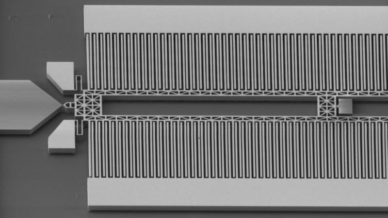
Lendway is developing a silicon actuator that is able to generate motion of just a few nanometers. This is achieved using an electrostatic comb drive that is suspended and held in position using several built-in springs. The structures in the video form what is known as an electromechanical system, which converts electrical signals into mechanical movement in a similar way to a conventional electric motor. Unlike motors, however, which are primarily used to transmit power, miniaturized versions of electromechanical systems are often used as high-precision sensors – for example in vehicles to measure acceleration, rotation or position. Their strength lies less in the generation of large movements and more in the fine control and detection of the smallest changes. Lendway's system works with movements at the lower limit of what is possible, with precision and control down to individual nanometers. The researcher wants to use this to apply mechanical tension to quantum materials such as graphene, graphene nanoribbons (GNRs) and carbon nanotubes (CNTs).
"Calculations and simulations in theoretical physics show that, under mechanical stress, these carbon-based nanomaterials could acquire novel electronic, optical and mechanical properties," explains Lendway. "However, so far hardly anyone has succeeded in demonstrating these effects experimentally – especially under cryogenic conditions. Measurements at very low temperatures are an essential prerequisite for most applications in quantum technology." Deforming quantum materials just a few nanometres in size in a controlled manner without damaging them, and measuring their properties at the same time is no easy task. As part of his doctorate at the Department of Information Technology and Electrical Engineering (D-ITET) of ETH Zurich, Lendway is developing a platform that will make this possible. His work is supported by the Swiss National Science Foundation (SNSF) and the State Secretariat for Education, Research and Innovation (SERI).
With high precision
The system in the video is one of several systems Lendway has developed for different types of nanomaterials. All systems use an electrostatic actuator in which capacitors are arranged in several rows like the teeth of a comb. Two of these comb-like structures interlock without touching each other. Voltage is applied to one of the combs – visible in the video as a dark discoloration. This causes the charged and uncharged combs to attract each other. A stopper at one end of the actuator ensures that the movement does not exceed 200 nanometers. As soon as the voltage is reduced, a springs return the actuator to its starting position. The system in the video is designed to contact individual molecules. For this purpose, there is a fine bridge of pure gold at the left end of the structure that can be broken to form atomically sharp electrodes.
The high-precision manufacturing of the tiny electromechanical systems is demanding. A single speck of dust, a hair – and the entire system is out of order. This is why Lendway fabricates the electromechanical devices in the clean room at the Binnig and Rohrer Nanotechnology Center (BRNC) of IBM, ETH Zurich and Empa in Rüschlikon. They are then transported to Empa under a protective atmosphere to carry out the experiments. It takes around ten days to produce a chip, which can hold between 54 and 74 such systems.
Lendway's project is not yet complete. "We have successfully developed various platforms, each of which is suitable for a different nanomaterial. Now we are starting to investigate their properties," says the researcher. Their findings could one day contribute to the development of nanoscale electronic components with new characteristics, which would open up possibilities in the fields of quantum technologies and more efficient energy use and help us better understand materials at a fundamental level.
